

 Description
 Specifications
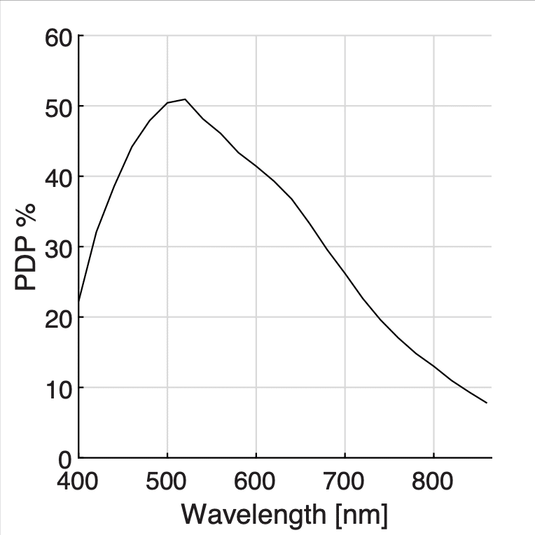
 QE Curve
 Applications
 Pictures
 Videos
 Downloads
 Publications
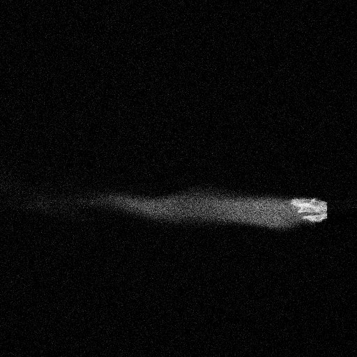
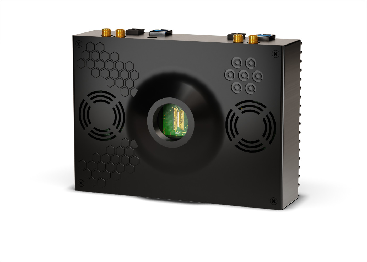
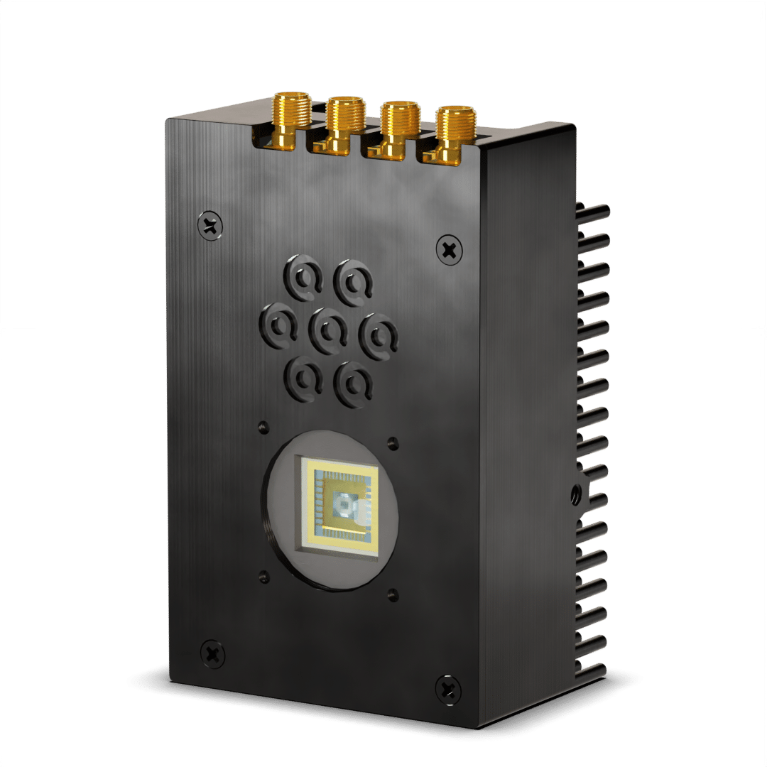
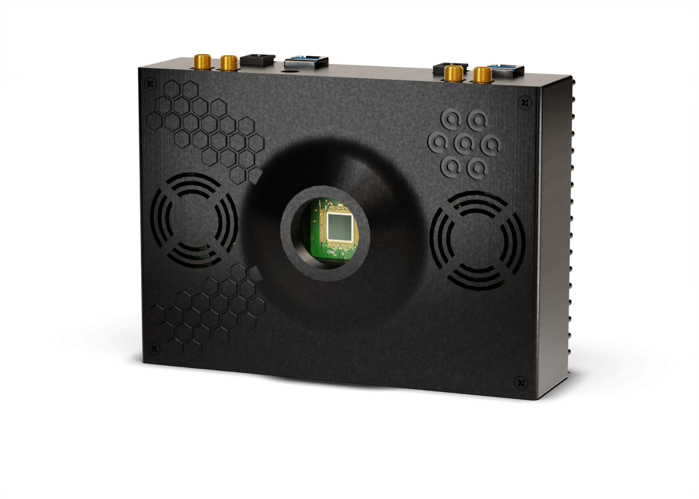
Photon-counting gated SPAD camera, in a nutshell
The SPAD512 and SPAD Alpha are photon-counting gated cameras based on a proprietary SPAD chip designed for single-photon sensitivity high-speed imaging. The core of these cameras is a SPAD image sensor with either a 512 x 512 array or a 1024 x 1024 array of pixels. It features a global shutter with picosecond precision and nanosecond exposures. It enables a peak photon detection probability of more than 50%, a typical dark count rate of less than 25 counts per second (SPAD512) and effectively zero readout noise.
The system software enables 1-bit, 4-bit, 6-bit, 7-bit, … up to 12-bit imaging with gated capability down to 6 ns with steps as small as 20 ps and phasor FLIM processing. It can be accessed through TCP/IP for easy integration into LabVIEW, Matlab, or Python.
Thanks to its single-photon sensitivity and gated capability the SPAD camera aims to replace EMCCD and ICCD is many experiments.
Photon-counting gated SPAD camera, more information
Intensity imaging
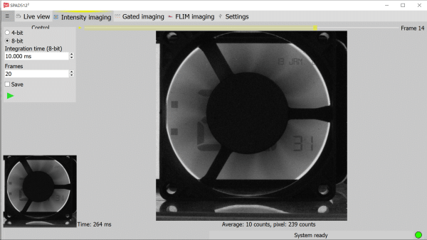
SPAD cameras delivers intensity images where the user defines the bit-depth, though these are obtained by sequentially summing 1-bit images. In a 1-bit image each pixel indicates whether it detected at least one photon (pixel value = 1) or none (pixel value = 0). Since the camera has only a single-bit memory in each pixel, incident photons might be ignored when the memory is already filled with a ‘1’. This effect is mainly noticeable for higher photon count rates and can be corrected, for instance using the pile-up correction. This correction transforms the measured amount of photons into the probable amount of photons that hit the SPAD. To correct the images, one can use the following formula to correct the measured number of photons in each pixel Nmeasured into the actual amount of photons Nactual:
This formula is valid for a 8-bit image data (255 levels). In case a different bit depth is used, the value 255 has to be adapted to reflect this change, e.g. 4-bit requires the value 15. For more information about the intensity imaging capabilities, please refer to the Software tab.
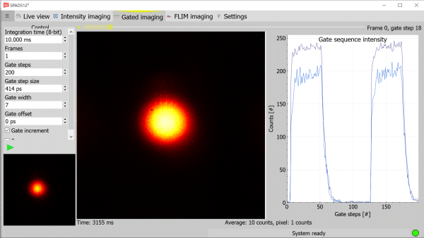
Gated imaging
SPAD cameras have gated imaging capabilities which provide some unique features similar to intensifiers. The SPAD gating measurement principle is explained below.
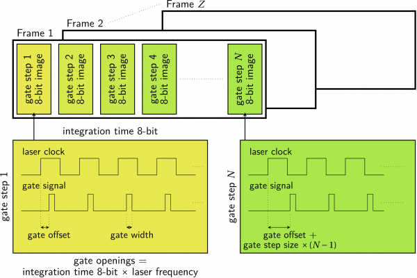
A gated frame is a series of 6, 7 or 8-bit images, each shifted by a small time step in order to reconstruct the time varying phenomenon of interest. The number of images to be taken in a single frame is given by the gate steps parameter, or in case arbitrary step sizes are used, by the number of arbitrary steps. Each step, the gate opening, defined by the gate width, is shifted by the set gate step in picoseconds. The gate is shifted away from the rising edge of the laser clock in either positive direction (gate increment) or negative direction (gate decrement). To create a single 8-bit image, the gate is opened for N times, where N is given by the integration time (8-bit) multiplied by the laser frequency. For example, when the integration time is set to 3ms and the laser frequency is 20MHz, the gate will open 60,000 times to create a single image. For more information about the gated imaging capabilities, please refer to the Software tab.
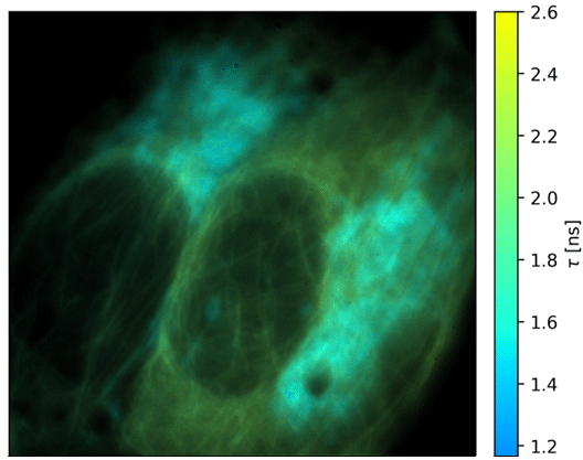
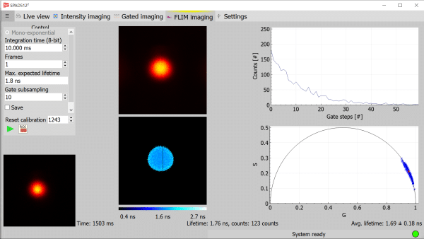
Fluorescence lifetime imaging
SPAD cameras also feature fluorescence lifetime imaging capabilities. This mode uses a sequence of gated images to calculate the lifetimes and generate a lifetime image. FLIM (Fluorescence Lifetime Imaging Microscopy) images are generated with the phasor method.
In the case of mono-exponential samples, the calibration of the IRF (Instrument Response Function) finds the falling edge of the gate. The end of the IRFs falling edge determines the starting point for normal measurements and the measurement window is defined by the maximum lifetime. Since the gate falling edge is convolved with the fluorescence decay for normal measurements, we will capture exactly the exponential part of the decay curve. The phasor is calculated directly from the measurement data without further corrections.
In the case of bi-exponential data, the calibration and measurements rely on the complete gate window. Therefore, the calibration determines both the gate rising and falling edges and calculates the complete window, including the extension from the fluorescence convolution. For normal measurements, the phasor data is calculated and the IRF phasor data is subtracted from it.
For each measurement, an intensity image, lifetime image, pixel response curve and phasor plot are generated. For more information about the fluorescence lifetime imaging capabilities, please refer to the Software tab.
What is a SPAD or single-photon avalanche diode ?
A single-photon avalanche diode or SPAD is a solid-state photodetector based on a reverse biased semi-conductor p-n junction like photodiodes and avalanche photodiodes (APDs), but unlike regular photodiodes, a SPAD operates in a mode called “Geiger mode” where a single incoming photon will create an electron-hole pair which will be amplified enough to create a measurable current. Therefore SPADs are intrinsically able to detect single-photons, with a very high temporal resolution.
The key component of a SPAD is a region within the diode called the depletion region. This region is designed to have a high electric field, which allows it to function as a high-gain avalanche photodiode. When a single photon interacts with the depletion region, it generates an electron-hole pair. The high electric field across the depletion region causes the electron and hole to accelerate, leading to a process known as impact ionization in which each electron or hole can gain enough energy to generate another electron-hole pair, resulting in an avalanche effect. This avalanche process rapidly amplifies the initial signal, converting the weak optical signal from the single photon into a detectable electrical pulse.
SPADs can be compared to other single-photon detection technologies such as PMTs and APDs, but SPADs have several advantages over those two type of detectors.
Compared to photomultiplier tubes (PMTs), SPADs have:
- higher sensitivity over wider spectral range ;
- better time resolution ;
- less bulky so more suitable for assembling into large arrays ;
- less sensitive to electromagnetic or mechanical perturbations.
Compared to avalanche photodiodes (APDs), SPADs have:
- higher detection efficiency ;
- smaller active areas ;
- generate less dark counts.
What is a SPAD camera ?
A SPAD camera refers to an arrangement of multiple single-photon avalanche diodes (SPADs) that are integrated into a two-dimensional rows and columns format. Each SPAD within the array operates independently and is capable of detecting individual photons. The SPAD camera combines the sensitivity and photon-counting capabilities of SPADs with the ability to detect photons across a larger spatial area.
Each SPAD in the camera array is assigned a unique address, allowing individual SPADs to be accessed and controlled independently. This addressing scheme enables selective readout of specific SPADs or groups of SPADs within the array, providing flexibility in data acquisition and analysis.
The main advantage of using a SPAD array is the ability to perform spatially resolved photon detection. By detecting photons across multiple locations simultaneously, it allows for the capture of detailed spatial information about the incoming light. This is particularly useful in applications such as imaging, where the spatial distribution of photons can be used to construct images or maps.
To view more photon counting photos, click HERE.
To visit the manufacturer’s website, click HERE.
SPAD Applications
Confocal microscopy
SPAD arrays increase light collection and enable innovation in the field of laser-scanning confocal microscopy. This innovation finally leads to a sharper and brighter image with functional information about the underlying molecular function, interactions and environment. SPAD arrays provide the following advantages in confocal microscopy:
- Achieve super-resolution with a standard confocal microscope ;
- Increase light collection ;
- Increase imaging speed ;
- Reduce background noise.
Quantum information
Temporal photon correlations and photon number resolving (PNR) are fundamental to probing the quantum properties of light. SPAD arrays have an extremely low crosstalk and thus enable reliable measurements of second and third order photon correlations, as well as quantum random number generation for unbreakable encryption. SPAD arrays provide the following advantages in quantum information:
- Simplify setup with single-chip multi-channel detector ;
- Increase data rate with detector parallelization ;
- Photon number resolving (PNR) detection.
Fluorescence lifetime imaging microscopy (FLIM)
SPAD cameras increase the overall photon throughput compared to scanned detection systems from the typical 10 Mcounts per second to 26 Gcounts per second. SPAD cameras provide the following advantages in FLIM:
- Simplify FLIM setup ;
- Increase FLIM frame rate.
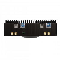
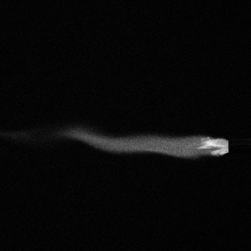
High-speed imaging
SPAD cameras enable high frame rates with global shutter at zero readout noise. SPAD cameras provide the following advantages in high-speed imaging:
- Image fast phenomena in low light conditions ;
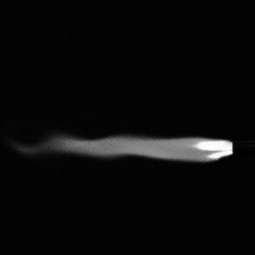
- Image light-in-flight.
Publications
- Imaging With Very Few Photons: EMCCD, SCMOS, And SPAD Detectors
- Imaging And Measuring Fluorescence Lifetime With The SPAD512S Camera
Publications about & with SPAD:
White Papers about SPAD512:
- Comparison between SPAD and EMCCD Cameras in Low-Light Conditions. Maxime Berchet, Cyril Saudan, Michel Antolovic. May 2025.
Quantum Information:
- Metasurface for programmable quantum algorithms with classical and quantum light. Randy Stefan Tanuwijaya, Hong Liang, Jiawei Xi, Wai Chun Wong, Tsz Kit Yung, Wing Yim Tam, and Jensen Li. De Gruyter. February 2024.
- Continuous heralding control of vortex beams using quantum metasurface. Hong Liang, Hammad Ahmed, Wing Yim Tam, Xianzhong Chen & Jensen Li. Nature Communications Physics. June 2023.
Widefield Fluorescence Lifetime Imaging Microscopy:
- Fast volumetric fluorescence lifetime imaging of multicellular systems using single-objective light-sheet microscopy. , , , , , , , , , , , , , ,
- Multiplexed near infrared fluorescence lifetime imaging in turbid media. Meital Harel, Uri Arbiv & Rinat Ankri. SPIE. February 2024.
- Au nanodyes as enhanced contrast agents in wide field near infrared fluorescence lifetime imaging. Neelima Chacko, Menachem Motiei, Jadhav Suchita Suryakant, Michael Firer & Rinat Ankri. Discover Nano. January 2024.
- Time-gated fluorescence lifetime imaging in the near infrared regime; A comprehensive study toward in vivo imaging. ,
Light-In-Flight Imaging:
-
Time-resolved laser speckle contrast imaging (TR-LSCI) of cerebral blood flow. Faraneh Fathi, Siavash Mazdeyasna, Dara Singh, Chong Huang, Mehrana Mohtasebi, Xuhui Liu, Samaneh Rabienia Haratbar, Mingjun Zhao, Li Chen, Arin Can Ulku, Paul Mos, Claudio Bruschini, Edoardo Charbon, Lei Chen & Guoqiang Yu. arXiv. September 2023.
Publications with Swiss SPAD3 (first predecessor):
- NIR fluorescence lifetime macroscopic imaging with a novel time-gated SPAD camera. Xavier Michalet, Arin C. Ulku, Michael A. Wayne, Shimon Weiss, Claudio Bruschini & Edoardo Charbon. SPIE. April 2023.
Publications with SwissSPAD2 (second predecessor):
- In vitro and in vivo NIR fluorescence lifetime imaging with a time-gated SPAD camera. Jason T. Smith, Alena Rudkouskaya, Shan Gao, Juhi M. Gupta, Arin Ulku, Claudio Bruschini, Edoardo Charbon, Shimon Weiss, Margarida Barroso, Xavier Intes, & Xavier Michalet. Optica. May 2022.
- Light detection and ranging with entangled photons. Jiuxuan Zhao, Ashley Lyons, Arin Can Ulku, Hugo Defienne, Daniele Faccio & Edoardo Charbon. Optics Express. January 2022.
- Full-field quantum imaging with a single-photon avalanche diode camera. Hugo Defienne, Jiuxuan Zhao, Edoardo Charbon & Daniele Faccio. Physical Review A. April 2021.
- Wide-field time-gated SPAD image for phasor-based FLIM applications. Arin Ulku, Andrei Ardelean, Michel Antolovic, Shimon Weiss, Edoardo Charbon, Claudio Bruschini & Xavier Michalet. IOP Science. February 2020.
- A 512×512 SPAD image sensor with integrated gating for widefield FLIM. Arin Can Ulku, Claudio Bruschini, Ivan Michel Antolović, Yung Kuo, Rinat Ankri, Shimon Weiss, Xavier Michalet & Edoardo Charbon. IEEE Journal of Selected Topics in Quantum Electronics. August 2018.
Publications with SwissSPAD (third predecessor):
- SPAD imagers for super resolution localization microscopy enable analysis of fast fluorophore blinking. Ivan Michel Antolovic, Samuel Burri, Claudio Bruschini, Ron A. Hoebe & Edoardo Charbon. Nature Scientific Reports. March 2017.
Other publications about SPAD technology:
- Megapixel time-gated SPAD image sensor for 2D and 3D imaging applications. Kazuhiro Morimoto, Andrei Ardelean, Ming-Lo Wu, Arin Can Ulku, Ivan Michel Antolovic, Claudio Bruschini & Edoardo Charbon. Optica. April 2020.
- Single-photon avalanche diode imagers in biophotonics: review and outlook. Claudio Bruschini, Harald Homulle, Ivan Michel Antolovic, Samuel Burri & Edoardo Charbon. Nature. September 2019.