In the realm of advanced imaging, SWIR (Short-Wave InfraRed) microscopy stands out as a powerful tool that pushes the boundaries of what we can see. While traditional optical microscopy is limited to the visible spectrum and NIR (roughly 400-1000 nm), SWIR microscopy operates in the infrared range from about 900 nm to 1700 nm—sometimes extending up to 2500 nm with specialized sensors. This allows scientists, engineers, and researchers to peer into materials and processes that are opaque or invisible under visible light. By capturing photons in this wavelength band, SWIR microscopy reveals hidden details, from complex structures in semiconductor materials to deep-tissue biological interactions. In this blog post, we’ll dive deep into what SWIR microscopy is, the cameras and optics involved and its key applications.
What is SWIR Microscopy and How Does It Work?
SWIR refers to the short-wave infrared portion of the electromagnetic spectrum, where light behaves similarly to visible light in terms of reflection and absorption but with unique advantages. Unlike thermal imaging (which detects heat in longer infrared wavelengths), SWIR imaging relies on reflected light, producing high-contrast, shadow-rich images that resemble black-and-white photographs. This makes it ideal for microscopy, where precision and detail are paramount.
At its core, SWIR microscopy works by illuminating a sample with SWIR light sources—such as lasers, LEDs, or broadband lamps—and capturing the reflected or transmitted light. The key principle is the inner photoelectric effect: incoming photons are absorbed by a sensor material, generating electron-hole pairs that create a measurable electric current. This process is highly efficient in SWIR due to lower scattering in tissues, and the ability to penetrate materials like silicon, glass, plastics, textiles and fabrics, biological tissues, some liquids etc.
Compared to visible or near-infrared (NIR) microscopy, SWIR offers deeper penetration and less autofluorescence (unwanted background glow from samples), making it perfect for non-destructive analysis. For instance, it can detect moisture content, chemical compositions, or defects without altering the sample.
The Key Components: Cameras and Optics in SWIR Microscopy
To build a SWIR microscopy system, you need specialized hardware that can handle these longer wavelengths. Standard silicon-based cameras (like CCD or CMOS sensors) fall short because they aren’t sensitive enough beyond about 1100 nm. Here’s a breakdown of the essential components:
Cameras
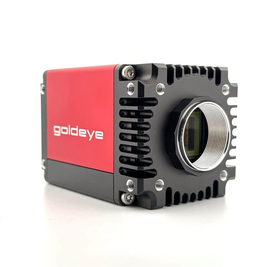
SWIR cameras are the heart of the system, typically built around Indium Gallium Arsenide (InGaAs) sensors. These sensors use a P-I-N photodiode structure (P-type semiconductor, intrinsic layer, N-type semiconductor) to efficiently convert SWIR photons into electrical signals. InGaAs is preferred for its high quantum efficiency, low noise, and ability to operate at room temperature—though cooling (via thermoelectric coolers, water, or even liquid nitrogen) is often added to minimize dark current and readout noise for high-sensitivity applications.
Things to consider when picking a SWIR camera for SWIR microcopy applications:
pixel size: the pixel size of a camera sensor directly influences the resolution on the sample, but it’s only one part of a complex interplay involving the microscope’s optics, magnification, and the sample’s properties. Here’s a clear explanation of how pixel size relates to resolution on the sample:In microscopy, the pixel size of a camera sensor directly influences the resolution on the sample, but it’s only one part of a complex interplay involving the microscope’s optics, magnification, and the sample’s properties.
Here’s a clear explanation of how pixel size relates to resolution on the sample
The resolution on the sample is determined by the microscope’s optical resolution, which depends on the numerical aperture (NA) of the objective lens and the wavelength (λ) of light used. The Rayleigh criterion for optical resolution is approximately:
Optical Resolution = 0.61 ⋅ λ / NA (λ = wavelength, NA = numerical aperture)
This gives the smallest resolvable distance on the sample (in the object plane). When this image is projected onto the camera sensor via magnification (M), the size of the resolvable feature on the sensor becomes:
Feature Size on Sensor = Optical Resolution ⋅ M
To capture this detail without losing information, the pixel size (P) on the sensor must be small enough to sample this feature adequately. According to the Nyquist criterion, the pixel size should be:
P ≤ Feature Size on Sensor / 2 = Optical Resolution ⋅ M /2
Or, equivalently, the pixel size in the sample plane (effective pixel size) is:
Effective Pixel Size on Sample = P / M
For optimal resolution, the effective pixel size on the sample should be at least half the optical resolution:
P /M ≤ Optical Resolution / 2 = 0.61⋅λ/(2⋅NA)
active area: the active area of a camera sensor (the total light-sensitive area, typically measured in millimeters) directly influences the field of view (FOV) on the sample, as it determines how much of the magnified image is captured. The relationship depends on the microscope’s magnification and optical system
Here’s a clear explanation of the active area relates to the field of view on the sample
The FOV on the sample is calculated by dividing the sensor’s active area by the total magnification of the microscope:
FOV on Sample (in mm) = Sensor Active Area (in mm) / Total Magnification
The total magnification includes the objective magnification (e.g., 40x) and any additional magnification from the tube lens or eyepiece (e.g., 1x or 1.5x). For example, a 40x objective with a 1x tube lens gives a total magnification of 40x.
Other parameters such as dark current and spectral range of the sensor should be considered when selecting a camera for SWIR microscopy. Extended SWIR (eSWIR) variants adjust the indium content in InGaAs to reach up to 2500 nm, grown epitaxially on InP substrates for broader spectral coverage. Alternatives like Mercury Cadmium Telluride (HgCdTe) exist but are less common due to higher costs.
Recommended products


Optics
Optics for SWIR microscopy must be transparent to infrared wavelengths, as standard glass lenses absorb SWIR light and cause aberrations. Specialized lenses use materials like germanium, chalcogenide glass, or calcium fluoride, often with anti-reflective coatings optimized for 900-1700 nm. Several off-the-shelf optical assemblies include:
Main components:
- SWIR camera
- Optional spectral filter
- SWIR coated zoom with magnification adjustment ring
- Optional coaxial illumination port (halogen or SWIR LED)
- Microscope objective
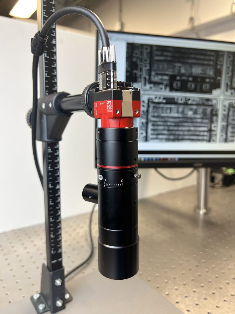
SWIR telecentric lenses combine the unique properties of telecentric optics with materials and coatings optimized for SWIR light, enabling high-precision imaging where standard visible-light lenses would fail due to poor transmission or aberrations. In a telecentric lens, the entrance or exit pupil is positioned at infinity, ensuring that light rays from the object are parallel to the optical axis. This eliminates perspective distortion and parallax errors, providing accurate size measurements of features at different distances and constant magnification across the entire field of view (FOV), regardless of object depth variations.
Field of view = Sensor active area / Magnification
Effective pixel size on sample = Pixel size / Magnification
Advantages of telecentric lenses:
- simple and cost-effective setup
- easily connects to a C-mount camera
- optional coaxial port for in-line illumination
- available with several magnification (0.5X, 0.7X, 1X, 2X and 4X)
Applications of SWIR Microscopy
Biomedical and Life Sciences
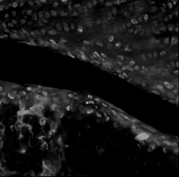
In biology, SWIR excels in the NIR-II window (1000-1700 nm), where tissue penetration is deeper and autofluorescence is minimal. It’s used for small animal imaging, tracking fluorophores like quantum dots or carbon nanotubes in real-time—e.g., visualizing mouse circulatory systems with Indocyanine nanoparticles. Applications include drug delivery monitoring, DNA sequencing, and studying deep-tissue interactions, reducing the need for invasive procedures
Photonics and Semiconductor Inspection
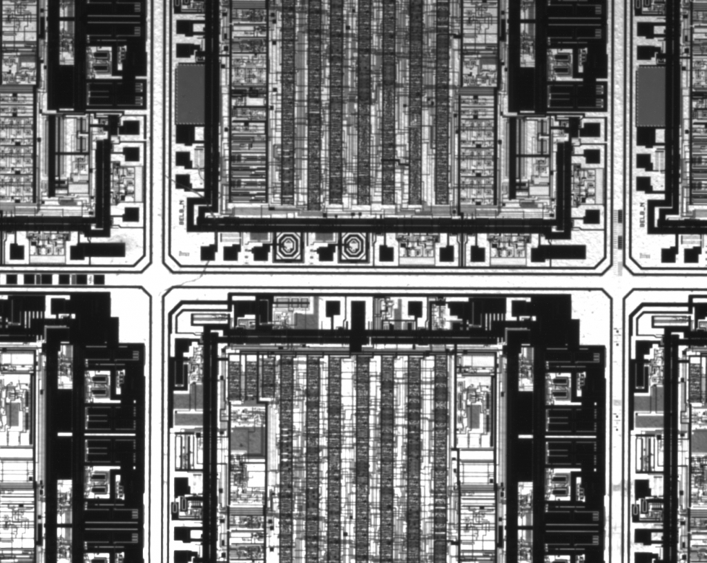
SWIR is crucial for silicon photonics, where integrated circuits use SWIR wavelengths for data transmission. It enables precise alignment, packaging, and defect detection in 2.5D/3D ICs, MEMS devices, and photonic chips (PICs or photonics on chips)
Materials Science and Research
Researchers use SWIR microscopy to analyze nanomaterials like graphene and carbon nanotubes, detecting unique spectral signatures. In hyperspectral imaging, it characterizes plastics or minerals, aiding geology and environmental monitoring.