Parallel optics can be challenging to characterize with classical fizeau interferometers. As a matter of fact, when both rear and front surfaces are parallel, multiple competitive interferograms can be observed, making a final interpretation impossible.
To solve this issue, Imagine Optic patented the POP method. An acronym for ‘Parallel Optics Procedure’, the POP method allows extracting the wavefronts reflected (RWE) from each individual surface (front and rear) as well as the transmitted wavefront error (TWE) by performing only two measurements. Unlike other techniques, the surfaces of the samples do not need to be modified to eliminate one of the reflections.
This new method is integrated on Imagine Optic’s metrology instrument MESO and its dedicated software, WaveSurf. Therefore, they are offering a solution providing both reflexion, transmission and POP measurements. This procedure is not only a revolution for interferometry applications, but a considerable time-saver: it takes only one minute to get your results, including calibration!
This blog post first presents the POP procedure and then illustrates it with the results of the characterization of a 6-inch glass wafer.
The POP procedure: the patented solution for thin plane parallel optics characterization
POP procedure: 2 steps – 3 wavefronts
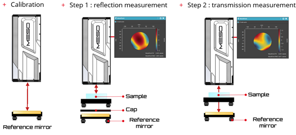
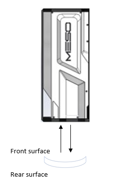
The POP procedure consists of a calibration and two steps (Figure 1.). The MESO instrument is set-up vertically for easy sample mounting and adjustment. This setup is typically used for glass wafer characterization.
– Calibration: A reference flat mirror is positioned in front of MESO. The software guides the user to finely align it. The measurement is automatically saved and the calibration is done.
– Step 1: This step is dedicated to the reflection measurement. It consists of aligning the sample: the reference mirror is covered with a black cap so the instrument only sees reflection from the sample, the sample is installed and the software helps the user to finely adjust its angle. The reflection measurement is done.
– Step 2: This step is dedicated to the transmission measurement. The only thing to do here is remove the cap in front of the reference mirror. The transmission measurement is done.
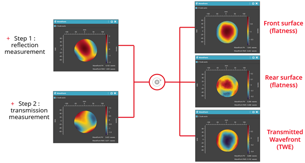
Then, the software processes the data and delivers three wavefronts: the front surface, the rear surface and the transmitted wavefront. (Figure 2.)
From only two measurements (reflection and transmission), MESO provides three error maps (TWE and RWE of both surfaces of the sample):
POP revolution: 4 key features
The POP method offers the following advantages:
– Insensitivity to rear surface reflections: the measurement is insensitive to reflections from the rear surface of the sample. Therefore, it is not necessary to modify the sample surface, avoiding additional handling, preparation, and subsequent cleaning that take time and affect the sample integrity.
– No sample handling during characterization: The sample does not need to be touched during the characterization procedure. Specifically, there is no need to flip the sample to measure both faces. This ensures perfect alignment of the obtained error maps without the need for fiducial markers.
– Versatility in wavelength: The POP method does not rely on absorbing the illumination beam to eliminate rear surface reflection (e.g., by working in the ultraviolet). Thus, characterization can be performed at any wavelength of interest, including the sample’s operating wavelength. MESO is available with up to 4 embedded sources.
– Low reflection coefficient compatibility: It allows for the characterization of samples with a reflection coefficient as low as 1%.
In the following, we will follow the POP procedure to characterize a 6” glass wafer.
Characterization of a 6-inch glass wafer
Glass wafer characterization – setup
The glass wafer has the following characteristics:
- Reference sample: WA1121 Corning
- Diameter : 6-inch
- Thickness: 1.1mm
- Material: Glass Uncoated
- Coefficient reflection surface: 0.04
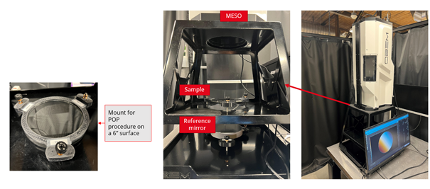
The sample was placed in a dedicated mount which allows accurate control of tip and tilt. The alignment of the reference mirror during the calibration and the alignment of the sample during Step 1 consist both in adjusting tip and tilt so the reflected light can get through a pinhole and be captured on the high resolution wavefront sensor of the MESO system.
Glass wafer characterization – results
The measurements are taken at a wavelength of 632.8 nm over a diameter of 150 mm. The measurement results obtained by the POP method for the wafer sample are as follows:
Front surface
The front surface flatness measured at 632 nm is 4.11 RMS waves, including -6 waves of curvature (in red on Fig. 5 – left). This means the entrance face of the wafer is slightly concave from the instrument’s point of view.
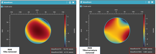
without tilt (left side) and without tilt and curvature (right side)
Rear surface
The flatness measured at 632 nm is 2.99 RMS waves, including +4 waves of curvature (in blue on Fig. 5 – left). This means the second surface of the wafer would be slightly concave if it was directly in front of the instrument.
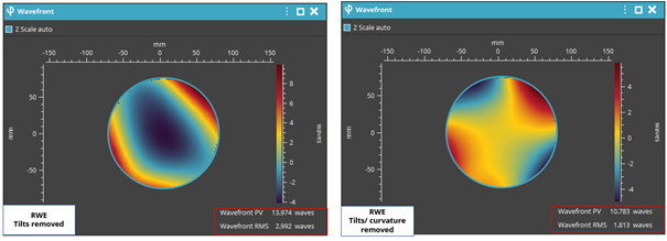
The front and the rear surfaces shapes given by the Wavesurf software confirms that they are parallel as shown on Figure 8.
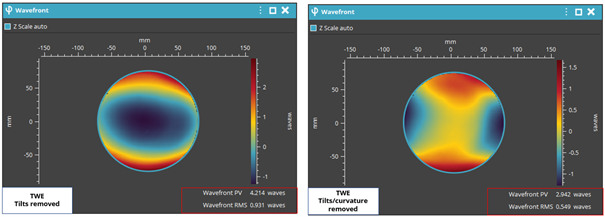
Transmission
Given that both faces are parallel, the transmitted wavefront error through the glass is expected to be low. It is observed that the residual wavefront error (filtering tilts) is 0.9 waves nm RMS (see Figure 7 – left). This corresponds to the difference in curvature measured between the two faces, considering the optical index of the glass. Ultimately, the transmission quality of this wafer is good
High orders – LIFT revolution
Thanks to the software Wavesurf and Imagine Optic’s LIFT algorithm which increase the resolution by a factor of 16, the user can filter all orders (Zernike up to 100) and detect defects, polishing residues, or scratches. (Figure 10. – left).
Looking only at high spatial frequencies, we measure 0.008 waves RMS which shows a high quality glass wafer (see Figure 10 – right).
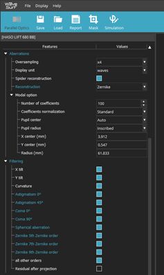
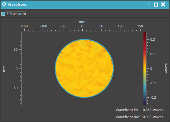
Figure 9: Screenshots from WaveSurf software from Imagine Optic showing the filtering of Zernike coefficients (left) and the residual wavefront (right)
3. Conclusion
The POP procedure developed by Imagine Optic, implemented in their MESO instrument, is a revolution for plane parallel optics metrology. Combining two high resoluted measurements, the dedicated Software Wavesurf delivers in one minute three wavefronts : the front surface, the rear surface and the transmitted wavefront.
This procedure represents a revolution for plane parallel optics metrology such as the 6-inch glass wafer presented in this blog post. The results are not only done in less than a minute but provided with a high resolution (680 x 500 phase point resolution) and accuracy (λ/100 RMS).
MESO is a unique instrument that can measure at multiple wavelengths (up to 4), enabling high resolution characterization of a wide range of flat optics such as glass wafers, filters, mirrors, crystals, and more.
Fore more information on MESO metrology system click here.
For more information on wavefront sensors and metrology systems, click here.